
TITAC-2 is a 32-bit asynchronous (clock-free) microprocessor whose architecture has been borrowed from the MIPS R2000 processor, including five-stage pipeline, on-chip cache, exception handling, external interruption and memory protection, although the object code is not compatible because of a different instruction encoding. Main modifications are multiple/divide, privilege instruction and delay slots of branch instructions. The TITAC-2 chip has been fabricated using 3 layer metal, 0.5 micron rule CMOS standard cell technology, integrating 496,367 MOS transistors and 8.6K Byte memory macro in 12.15 mm x 12.15 mm.
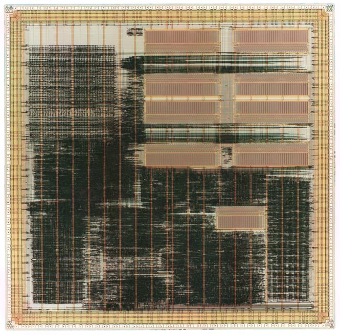 This is the final layout of TITAC-2 microprocessor.
The final tape was sent out on the Christmas Eve of 1996.
The TITAC-2 chip was fabricated by
NEC Corporation.
It returned from
fabrication on Feb.15, 1997. After one-week step-by-step debugging for
the processor board including memory, I/O, and other miscellaneous circuits
for evaluation experiments, the TITAC-2 chip ran the Dhrystone V2.1
benchmark program successfully on Feb.22, 1997.
This is the final layout of TITAC-2 microprocessor.
The final tape was sent out on the Christmas Eve of 1996.
The TITAC-2 chip was fabricated by
NEC Corporation.
It returned from
fabrication on Feb.15, 1997. After one-week step-by-step debugging for
the processor board including memory, I/O, and other miscellaneous circuits
for evaluation experiments, the TITAC-2 chip ran the Dhrystone V2.1
benchmark program successfully on Feb.22, 1997.
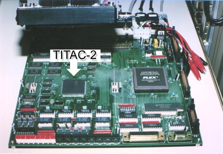 This is the experimental board on which the TITAC-2 processor is mounted as
well as 512K-byte SRAM, 128K-byte EPROM, I/O contol logic and
miscellaneous circuits for evaluating performance, delay-insensitivity,
power consumption.
This is the experimental board on which the TITAC-2 processor is mounted as
well as 512K-byte SRAM, 128K-byte EPROM, I/O contol logic and
miscellaneous circuits for evaluating performance, delay-insensitivity,
power consumption.
The TITAC-2 works correctly with its power supply voltage being varied through the range from 1.5 V to 6.0 V and the temperature of its package surface being heated up to about 85 degrees Celsius by hair dryer and cooled down with liquid nitrogen, and achieves 54 VAX MIPS using the Dhrystone benchmark with a power consumption of 2W at 3.3 V for room temperature .
A significant feature of the design is the introduction of a new delay model, called the Scalable-Delay-Insensitive (SDI) model, which provides with a reasonable approach to dependable and high-performance asynchronous VLSI system design. The SDI model is an unbounded delay model, i.e. no upper bound is assumed on the gate and wire delays. Unlike the well-known Delay-Insensitive (DI) model, the SDI model assumes that a bound exists on the variation ratio of the relative delay between any two components. An SDI circuit operates correctly even if the "actual" delay of a signal propagation path in the circuit becomes K times larger than the "estimated" delay, thus achieving a sufficient degree of delay-insensitivity, and operates much faster than the DI or Quasi-DI counterpart. In the TITAC-2 design, by taking account of the technology used, the entire system was divided into sub-circuits with each sub-circuit being limited within a maximum of 1.93mm x 1.93mm, which validates that the maximum variation ratio K is determined to be 2. Then, each sub-circuit was designed based on the SDI model with K=2, while global interconnection between subcircuits was designed based on the DI model.